Difference between revisions of "PAL16L8"
(→See also) |
(→PAL I/O port) |
||
| (24 intermediate revisions by the same user not shown) | |||
| Line 5: | Line 5: | ||
== Fixed version (Gerald) == | == Fixed version (Gerald) == | ||
Original version from Porchy suffer from a bad handling of the RAMDIS signal. This cause screen artefact when accessing an external extension RAM like XMEM. | Original version from Porchy suffer from a bad handling of the RAMDIS signal. This cause screen artefact when accessing an external extension RAM like XMEM. | ||
| − | |||
A14OUT = !( !A14 | A14OUT = !( !A14 | ||
| Line 89: | Line 88: | ||
[[File:Amstrad6128.jed]] Original JED File posted on CPCWiki Forum | [[File:Amstrad6128.jed]] Original JED File posted on CPCWiki Forum | ||
| − | == | + | == PAL MMR register == |
| + | This register controls how the extended RAM is banked into the CPU address space. It doesn't affect the video display at all as the Gate Array can only access the Base 64k page of RAM. | ||
| − | + | {|{{Prettytable|width: 700px; font-size: 2em;}} | |
| + | |colspan=2|'''MMR'''||colspan=3|'''64K page'''||'''S'''||colspan=2|'''MM'''||colspan=4 style="text-align: center;"|'''CPU Memory Mapping''' | ||
| + | |- | ||
| + | |'''7''' | ||
| + | |'''6''' | ||
| + | |'''5''' | ||
| + | |'''4''' | ||
| + | |'''3''' | ||
| + | |'''2''' | ||
| + | |'''1''' | ||
| + | |'''0''' | ||
| + | |style="text-align: center;"|'''&0000-&3fff''' | ||
| + | |style="text-align: center;"|'''&4000-&7fff''' | ||
| + | |style="text-align: center;"|'''&8000-&bfff''' | ||
| + | |style="text-align: center;"|'''&c000-&ffff''' | ||
| + | |- | ||
| + | |1 | ||
| + | |1 | ||
| + | |colspan=3 style="text-align: center;"|x | ||
| + | |0 | ||
| + | |0 | ||
| + | |0 | ||
| + | |Base 64k / Bank 0 | ||
| + | |Base 64k / Bank 1 | ||
| + | |Base 64k / Bank 2 | ||
| + | |Base 64k / Bank 3 | ||
| + | |- | ||
| + | |1 | ||
| + | |1 | ||
| + | |colspan=3 style="text-align: center;"|p | ||
| + | |0 | ||
| + | |0 | ||
| + | |1 | ||
| + | |Base 64k / Bank 0 | ||
| + | |Base 64k / Bank 1 | ||
| + | |Base 64k / Bank 2 | ||
| + | |'''Page p / Bank 3''' | ||
| + | |- | ||
| + | |1 | ||
| + | |1 | ||
| + | |colspan=3 style="text-align: center;"|p | ||
| + | |0 | ||
| + | |1 | ||
| + | |0 | ||
| + | |'''Page p / Bank 0''' | ||
| + | |'''Page p / Bank 1''' | ||
| + | |'''Page p / Bank 2''' | ||
| + | |'''Page p / Bank 3''' | ||
| + | |- | ||
| + | |1 | ||
| + | |1 | ||
| + | |colspan=3 style="text-align: center;"|p | ||
| + | |0 | ||
| + | |1 | ||
| + | |1 | ||
| + | |Base 64k / Bank 0 | ||
| + | |'''Base 64k / Bank 3''' | ||
| + | |Base 64k / Bank 2 | ||
| + | |'''Page p / Bank 3''' | ||
| + | |- | ||
| + | |1 | ||
| + | |1 | ||
| + | |colspan=3 style="text-align: center;"|p | ||
| + | |1 | ||
| + | |colspan=2 style="text-align: center;"|b | ||
| + | |Base 64k / Bank 0 | ||
| + | |'''Page p / Bank b''' | ||
| + | |Base 64k / Bank 2 | ||
| + | |Base 64k / Bank 3 | ||
| + | |} | ||
| − | + | == PAL I/O port == | |
| + | |||
| + | Note that no settings are stored in the Gate Array regarding register 3, but the PAL and Gate Array share an I/O port address. | ||
| + | |||
| + | Bit14 of the PAL selection address can be at 0 or 1 on CPCs equipped with CRTCs 0, 1, 2. It must be at 1 on CRTCs 3 and 4. | ||
| + | |||
| + | For compatibility reasons, it is strongly advised to always set bit14 to 1 to select PAL. | ||
| + | |||
| + | == PAL Type Detection == | ||
| + | <pre> | ||
| + | 10 OUT &7F00,&C0:POKE &4000,&C0 | ||
| + | 20 OUT &7F00,&C7:POKE &4000,&C7:OUT &7F00,&C0 | ||
| + | 30 IF PEEK(&4000)=&C7 THEN PRINT"PAL chip absent/inactive":END | ||
| + | 40 OUT &BC00,&F:OUT &3DFF,&C7 | ||
| + | 50 IF PEEK(&4000)=&C7 THEN PRINT"PAL I/O layout on CRTC 0/1/2":END | ||
| + | 60 IF PEEK(&4000)=&C0 THEN PRINT"PAL I/O layout on CRTC 3/4":END | ||
| + | 70 PRINT"Error!" | ||
| + | </pre> | ||
| + | |||
| + | == See also == | ||
| + | |||
| + | *CPC 464/664 cannot deal with A14/A15 for Base 64k page like the 6128 does. So external RAM expansions differ in their behaviour regarding &C3 mode. See [https://www.cpcwiki.eu/forum/amstrad-cpc-hardware/464-preasic-c3-ram-configuration-and-rom-7/ Discussion on the forum] and [https://www.cpcwiki.eu/forum/amstrad-cpc-hardware/dk%27tronics-ram-c3-selection-464/ Another discussion] | ||
*[[Gate Array and ASIC Pin-Outs]] | *[[Gate Array and ASIC Pin-Outs]] | ||
| + | |||
| + | *[[Standard Memory Expansions]] | ||
[[Category:Datasheet]] | [[Category:Datasheet]] | ||
Latest revision as of 09:39, 14 May 2024
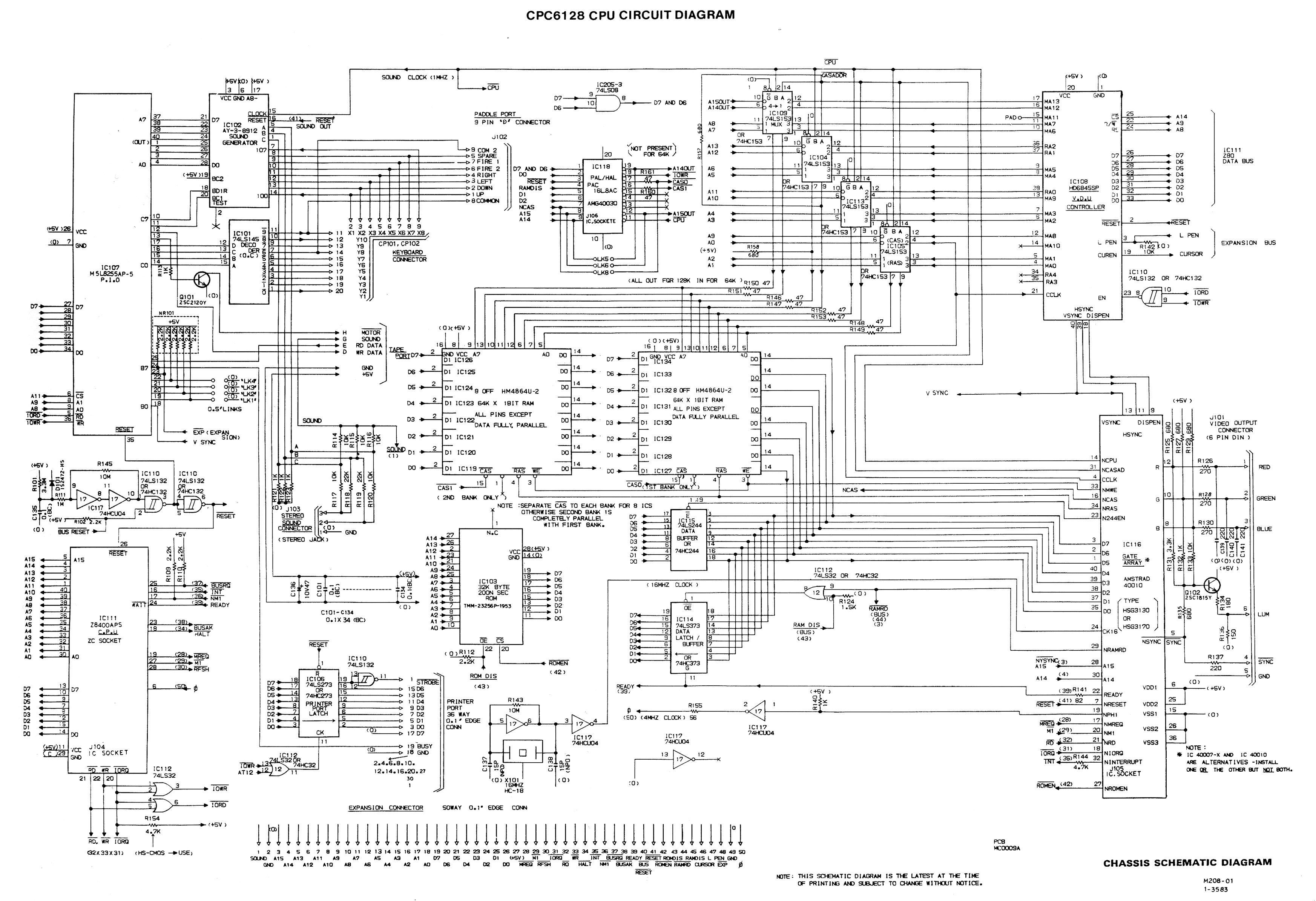
The CPC6128 second bank of 64K RAM is controlled by a PAL 16L8 chip. It has the Amstrad part number 40031.
On the CPC 6128 schematic, it is top centre: CPC6128 Schematic however the X inputs aren't distinguished.
Contents
Fixed version (Gerald)
Original version from Porchy suffer from a bad handling of the RAMDIS signal. This cause screen artefact when accessing an external extension RAM like XMEM.
A14OUT     = !(  !A14
             #   !A15 & !Q0 & Q2 );

A15OUT     = !(  !A15 & !A14
             #   !A15 & !Q1
             #   !A15 & !Q0 & !Q2 );

Q0     = (  D7ANDD6 & nRESET & D0 & !A15 & !nIOWR
         #   !D7ANDD6 & nRESET & Q0
         #   nRESET & A15 & Q0
         #   nRESET & nIOWR & Q0 );

Q1     = (  D7ANDD6 & nRESET & D1 & !A15 & !nIOWR
         #   !D7ANDD6 & nRESET & Q1
         #   nRESET & A15 & Q1
         #   nRESET & nIOWR & Q1 );

Q2     = (  D7ANDD6 & nRESET & D2 & !A15 & !nIOWR
         #   !D7ANDD6 & nRESET & Q2
         #   nRESET & A15 & Q2
         #   nRESET & nIOWR & Q2 );

nCAS0     = (  nCAS
            #   RAMDIS & !nCPU & nCAS0
            #   !A15 & A14 & !nCPU & Q2 & nCAS0
            #   A15 & A14 & !nCPU & Q0 & !Q2 & nCAS0
            #   !nCPU & !Q0 & Q1 & !Q2 & nCAS0
            #   !nCAS1 );

nCAS1     = !(  !RAMDIS & !nCAS & !A15 & A14 & !nCPU & Q2 & nCAS0
            #   !RAMDIS & !nCAS & A15 & A14 & !nCPU & Q0 & !Q2 & nCAS0
            #   !RAMDIS & !nCAS & !nCPU & !Q0 & Q1 & !Q2 & nCAS0
            #   !nCAS & !A15 & A14 & Q2 & nCAS0 & !nCAS1
            #   !nCAS & A15 & A14 & Q0 & !Q2 & nCAS0 & !nCAS1
            #   !nCAS & !Q0 & Q1 & !Q2 & nCAS0 & !nCAS1 );
File:CPC6128.JED : Fixed version of Amstrad 40031 GAL replacement
File:CPC6128.hex : Fixed version of Amstrad 40031 GAL replacement, Hex Intel version.
Initial replacement equation (Porchy)
The following equations were worked out by Porchy (member on CPCWiki Forum). These can be used to program replacements:
A15OUT = (!X2 & !X1 & A14
     # !X3 & !X2 & A14
     # A15);

!X1 = (!A15 & D7ANDD6 & RESET & !IOWR & D0
     # !X1 & RESET & IOWR
     # !X1 & !D7ANDD6 & RESET
     # !X1 & A15 & RESET);

!X2 = (!A15 & D7ANDD6 & RESET & !IOWR & D1
     # !X2 & RESET & IOWR
     # !X2 & !D7ANDD6 & RESET
     # !X2 & A15 & RESET);

!X3 = (!A15 & D7ANDD6 & RESET & !IOWR & D2
     # !X3 & RESET & IOWR
     # !X3 & !D7ANDD6 & RESET
     # !X3 & A15 & RESET);

!CAS1 = (X3 & !X1 & A15 & A14 & !NCAS & !RAMDIS & !CPU & CAS0
     # !X3 & !A15 & A14 & !NCAS & !RAMDIS & !CPU & CAS0
     # X3 & !X2 & X1 & !NCAS & !RAMDIS & !CPU & CAS0
     # !NCAS & CAS0 & !CAS1);

!CAS0 = (X3 & X2 & X1 & !NCAS & !RAMDIS & CAS1
     # X3 & !X1 & !A15 & !NCAS & !RAMDIS & CAS1
     # !X3 & A15 & !NCAS & !RAMDIS & CAS1
     # !X1 & !A14 & !NCAS & !RAMDIS & CAS1
     # !X3 & !A14 & !NCAS & !RAMDIS & CAS1
     # !NCAS & !RAMDIS & CPU & CAS1
     # !NCAS & !CAS0 & CAS1);

A14OUT = (A15 & A14
     # !X1 & A14
     # X3 & A14);
File:Amstrad6128.jed Original JED File posted on CPCWiki Forum
PAL MMR register
This register controls how the extended RAM is banked into the CPU address space. It doesn't affect the video display at all as the Gate Array can only access the Base 64k page of RAM.
| MMR | 64K page | S | MM | CPU Memory Mapping | |||||||
| 7 | 6 | 5 | 4 | 3 | 2 | 1 | 0 | &0000-&3fff | &4000-&7fff | &8000-&bfff | &c000-&ffff |
| 1 | 1 | x | 0 | 0 | 0 | Base 64k / Bank 0 | Base 64k / Bank 1 | Base 64k / Bank 2 | Base 64k / Bank 3 | ||
| 1 | 1 | p | 0 | 0 | 1 | Base 64k / Bank 0 | Base 64k / Bank 1 | Base 64k / Bank 2 | Page p / Bank 3 | ||
| 1 | 1 | p | 0 | 1 | 0 | Page p / Bank 0 | Page p / Bank 1 | Page p / Bank 2 | Page p / Bank 3 | ||
| 1 | 1 | p | 0 | 1 | 1 | Base 64k / Bank 0 | Base 64k / Bank 3 | Base 64k / Bank 2 | Page p / Bank 3 | ||
| 1 | 1 | p | 1 | b | Base 64k / Bank 0 | Page p / Bank b | Base 64k / Bank 2 | Base 64k / Bank 3 | |||
PAL I/O port
Note that no settings are stored in the Gate Array regarding register 3, but the PAL and Gate Array share an I/O port address.
Bit14 of the PAL selection address can be at 0 or 1 on CPCs equipped with CRTCs 0, 1, 2. It must be at 1 on CRTCs 3 and 4.
For compatibility reasons, it is strongly advised to always set bit14 to 1 to select PAL.
PAL Type Detection
10 OUT &7F00,&C0:POKE &4000,&C0
20 OUT &7F00,&C7:POKE &4000,&C7:OUT &7F00,&C0
30 IF PEEK(&4000)=&C7 THEN PRINT"PAL chip absent/inactive":END
40 OUT &BC00,&F:OUT &3DFF,&C7
50 IF PEEK(&4000)=&C7 THEN PRINT"PAL I/O layout on CRTC 0/1/2":END
60 IF PEEK(&4000)=&C0 THEN PRINT"PAL I/O layout on CRTC 3/4":END
70 PRINT"Error!"
See also
- CPC 464/664 cannot deal with A14/A15 for Base 64k page like the 6128 does. So external RAM expansions differ in their behaviour regarding &C3 mode. See Discussion on the forum and Another discussion