Difference between revisions of "CPC 6320 / CPC 6512 - internal 320K / 512K for CPC 6128"
m |
|||
| Line 99: | Line 99: | ||
| − | + | <br /> | |
| + | <br /> | ||
Revision as of 08:37, 29 October 2022
Contents
CPC 6320 - internal 320K for CPC 6128
The CPC 6128 can be upgrade to 320KB internally by replacing the 64Kbit ICs of the second RAM bank with 256Kbit ICs (41256) and the addition of a bit of logic to drive the new address line A8 of these RAM ICs.
The German magazine C'T had a similar idea in the 80s, however their expansion was not compatible with the dk'tronics standard and required to program a PAL while this expansion can be built with standard logic ICs and is fully compatible to dk'tronics.
The logic ICs are standard ICs which most "makers" probably have lying around. If not you can find them in any electronics store or on Ebay for cheap.
Warning / Disclaimer
Although I have taken the utmost care preparing this documentation, I am no electronics engineer and did this only as a hobby project. I do not guarantee that it is error free and I accept no responsibility for damage to anyone’s hardware or other personal equipment or injury inflicted on you or others.
Construction
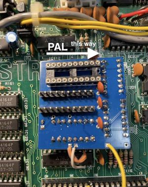
The required logic can either be built on a slim breadboard or with the help of a PCB that plugs into the PAL socket.
- 8x 41256 RAM IC, 150ns or faster
- 8x IC socket 16-pin (optional, but highly recommended)
- 1x 74HCT02 NOR gate
- 1x 74HCT32 OR gate
- 1x 40175 FlipFlop
- 1x IC socket, 20-pin (super flat, turned)
- 1x TriPad stripboard or PCB
- some wire
when using a TriPad stripboard:
- 2x IC socket 14-pin (optional, any will do it)
- 1x IC socket 16-pin (optional, any will do it)
- 3x capacitor 100nF
when using a PCB:
- 2x Pin header 1x10
- 4x capacitor 100nF
- optional: resistor 10k, switch
With the PCB you have to solder the ICs (except for the PAL) directly to the PCB as otherwise there is not enough headroom for the keyboard.
Preparation: Replace second RAM bank
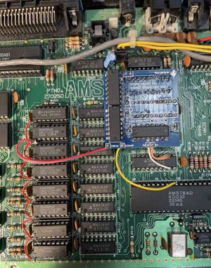
- desolder all RAM ICs of the second RAM bank (left one when looking from above). If you don't have the right tools to appropriately desolder the RAM ICs it can be easier to cut the legs and remove each leg. But of course, you will destroy the ICs with it.
- solder IC sockets into holes of the RAM ICs
- put RAM ICs into sockets
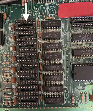
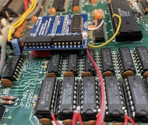
- connect pin 1 (A8) of each new IC together. Either on the backside of the motherboard or directly at pin 1 of the ICs (*)
(*) according to the schematics pin 1 should be unconnected on the motherboard. As this was different on e.g. a 464 and there are different revisions of the 6128 board it's better to check this on your motherboard. In case pin 1 is connected to GND or VCC, you have to bend up pin 1 so it's not connected to the socket and then connect pin1 of all ICs directly. This is shown in the picture here:
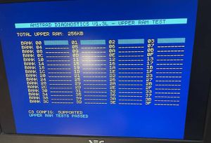
Now it's a good time to test if you have done everything right. Connect one of the A8 pins to GND with a wire and start the CPC. Run the diagnostics tool or a 128KB game. If you have done everything right, it should now behave exactly like a computer with 128KB built in.
Option A: TriPad stripboard
- Take a TriPad stripboard and cut out a part that is 2 stripes height has enough width to carry the 3 ICs plus capacitors.
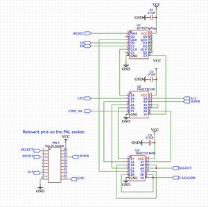
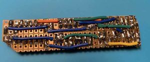
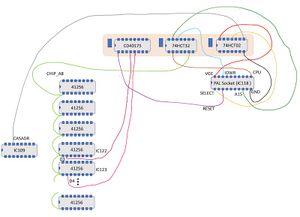
- solder the sockets to the stripboard according to the layout/schematics in the picture below
- solder the wires that go to other ICs on the mainboard to the stripboard
- now make all connections between the ICs according to the layout/schematics
- remove the PAL from its socket. Plug in another socket into the socket and solder all wires to their respective pins
- put the PAL into this socket
- finally connect the wires for chipA8, CASADR, D3 and D4 to the pins as documented in the diagram. (You can also use other soldering points as documented for the PCB below if they are more convenient.)
Option B: PCB
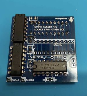
- solder the ICs and the capacitors to upper side the PCB
- if you want to disable the extension with a switch, also solder the resistor. The switch needs to be connected to the "disable" connection pads.
- if you have no intent to disable the extension, just bridge the "disable" connection pads with a wire. Don't populate the resistor.
- solder the PAL IC socket and the pin headers to backside of the PCB. The pin headers will later be pushed into the PAL socket on the motherboard. make sure they have quite the right length as if they are too long, there might not be enough headroom above the PCB for the keyboard and if they are too short, the connection might suffer.
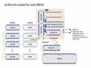
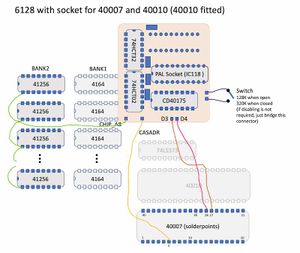
- connect chipA8 to one of the A8 pins of the new RAM chips and CASADR, D3 and D4 to appropriate connection points on the motherboard. The diagrams show some options. If you have mainboard with soldering points for the two different gate array versions, it's the most easiest way to use the soldering points there. Otherwise connections to IC pins are probably the easiest way.
important: double check wiring with actual Gate Array pinouts as the author of this article could not himself try alls options
(eto)
